Intel T1/E1 User Manual Page 12
- Page / 26
- Table of contents
- BOOKMARKS

- Quad T1/E1 Applications 1
- Contents 3
- 1.0 General Description 5
- 6 Developer Manual 6
- 2.0 Overview 7
- 2.4 Factory Settings 8
- 3.1 Power Connections 9
- 3.2 Hardware Mode Selection 9
- 3.3 Loopback Mode Selection 9
- 3.4 Clock Edge Selection 9
- 3.5 Output Enable Selection 10
- 3.6 Code Selection 10
- 3.9 Line Buildout Selection 11
- 3.10 Master Clock Setup 11
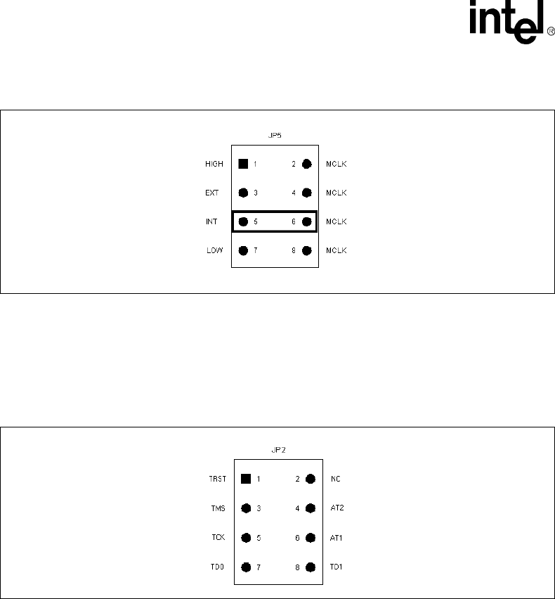
- 3.11 JTAG Boundary Scan Port 12
- 3.12 Framer/ASIC Connection 12
- 3.15 Board Protection 13
- 3.13 LED Indicators 13
- 3.14 Line Interface 13
- 4.2 Evaluation Board Set-up 14
- 4.4 Power Connections 14
- 4.5 Evaluation Board Software 15
- 4.7 Hardware Set-up Screen 15
- 4.8 Quitting the Program 15
- 4.9 Configuration Screen 16
- 4.9.4 Apply to all Channels 17
- 4.9.5 Exit 17
- 4.10 Registers Screen 18
- Developer Manual 19 19
- Figure 8. Registers Screen 19
- LEVEL ONE COMMUNICATIONS 20
- Developer Manual 21 21
- 22 Developer Manual 22
- Developer Manual 23 23
- 24 Developer Manual 24
- Developer Manual 25 25
Related products and manuals for Unknown Intel T1/E1
 (281 pages)
(198 pages)
(281 pages)
(198 pages)


 (84 pages)
 (2 pages) (1 pages)
(54 pages)
(53 pages)
(31 pages)
(23 pages)
(60 pages)
(13 pages)
(60 pages)
(2 pages) (1 pages)
(54 pages)
(53 pages)
(31 pages)
(23 pages)
(60 pages)
(13 pages)
(60 pages)
© 2020, manymanuals.com. All rights reserved. | 0.037 s |
 Manymanuals.com
 Manymanuals.de
 Manymanuals.fr
 Manymanuals.it
 Manymanuals.pl
 Manymanuals.cz
 Manymanuals.es
 Manymanuals-pt.com
Comments to this Manuals